Go to playground home.

PCB

This page contains improvements to the AWR Design Environment for PCB designers.

License requirements: Layout (MWO-XX5+) and either AXIEM (XEM-001) or Analyst (ANA-001)


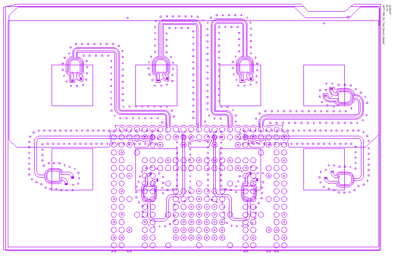
Easily cut out RF sections of interest for simulation.

Automatically cleanup PCB shapes for EM analysis.

Effortlessly add ports to PCB pads.

Analyze PCB EM structures faster than ever.
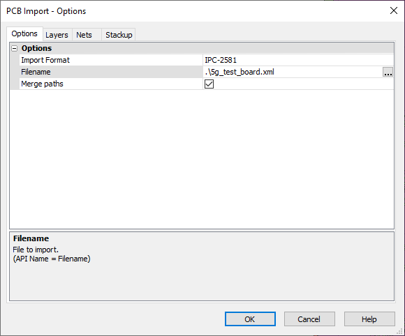

Importing the layout

The project will open ready to import the PCB.
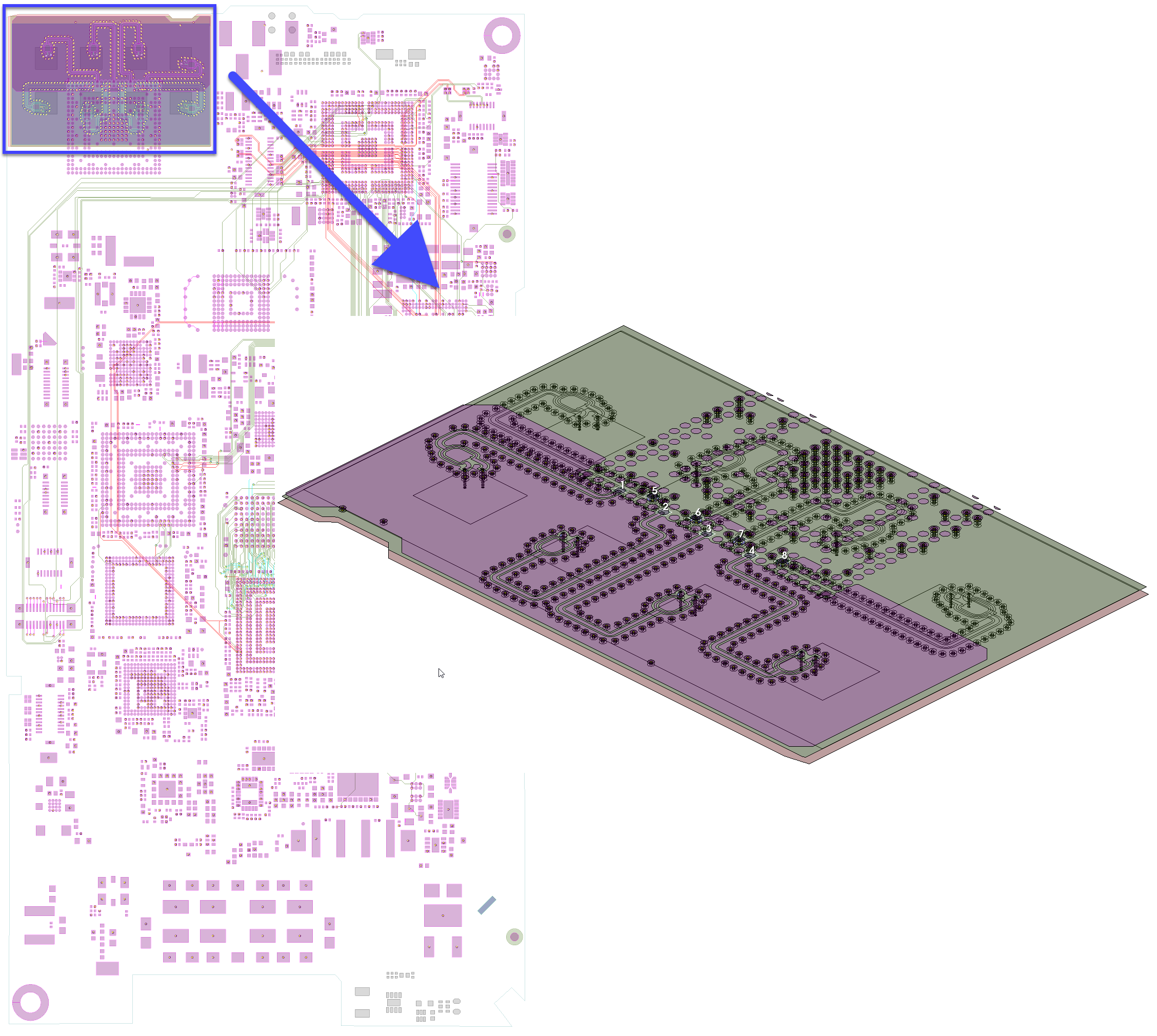
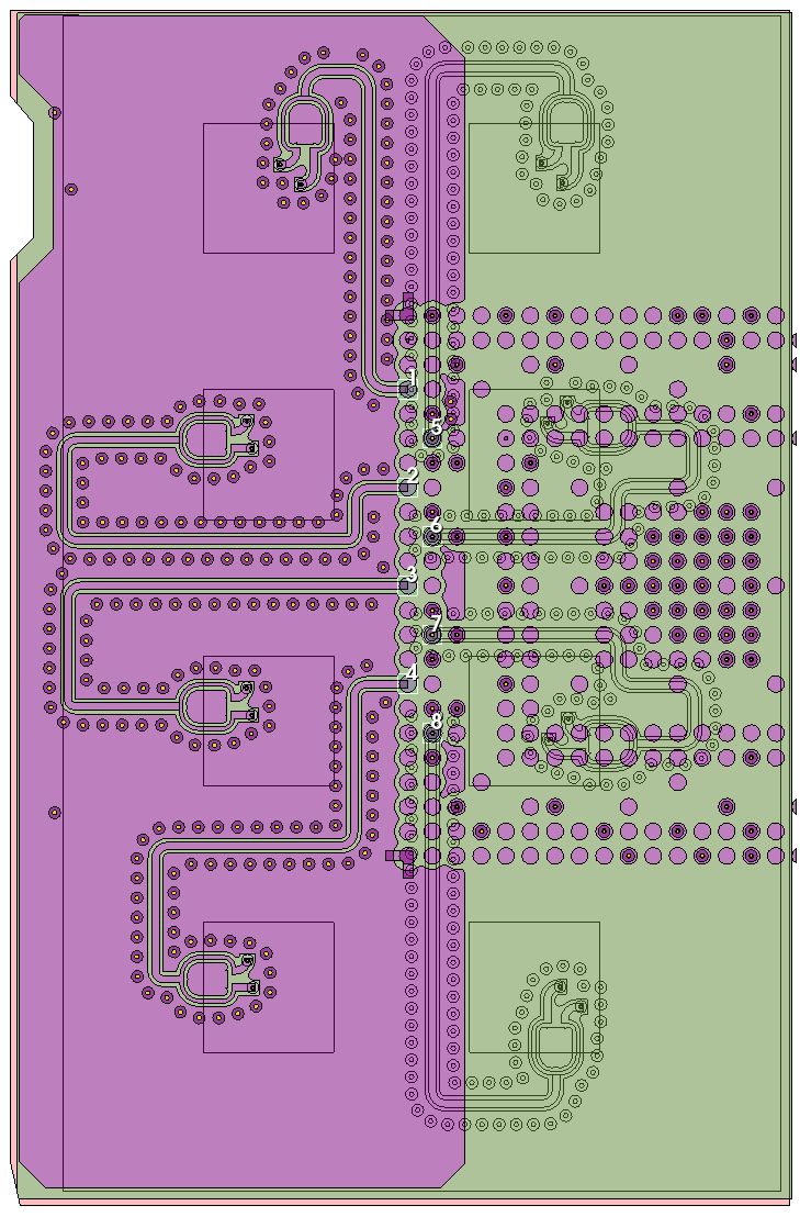
  1. Open the 5g_test_board instance of the PCB Import Wizard.
  2. Click on Import Format and note that the wizard supports both ODB++ and IPC-2581 files.
  3. Click through the tabs to show the control of which layers import, which nets import, and how the STACKUP imports.
    • STACKUP verification is important as often PCB export data doesn't contain the proper electrical properties.
  4. Press OK and the entire PCB will import and create a new Circuit Schematic called 5G_Test_Board

Cutting out the RF Region of Interest

Switches to already imported board to facilitate net selection.
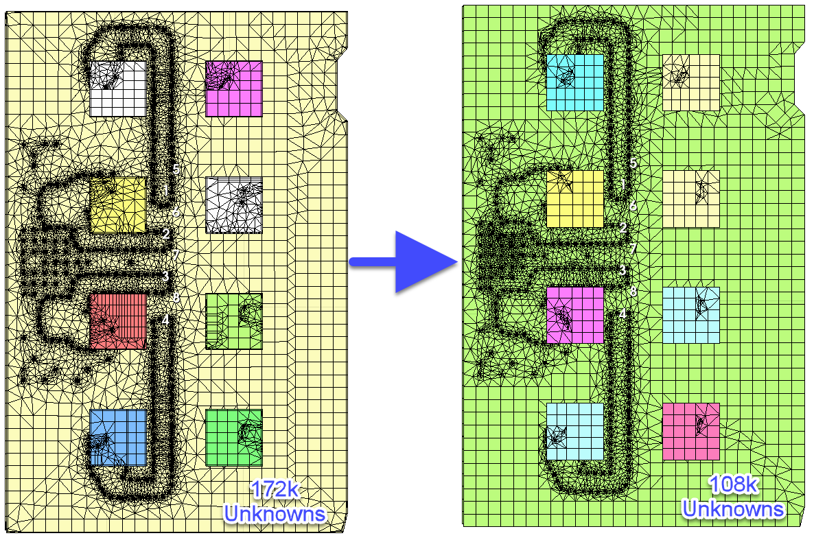
  1. Run the PCB EM Setup Wizard and choose Restore to restore the pin selection. Normally pin/net selection is done by the user but it was pre-saved in this example to make it easier to demo.
  2. Choose Smart Select to select the traces connected to these pins.
  3. Choose Smart Set Up to automatically create a ready to simulate EM Structure.
    • Choose Yes in the Create EM Clip Region dialog.
    • Choose Bounding Box and enter 2000um for the offset and click Preview then OK in the Create EM Clip Region Dialog
    • Choose Yes in the Layer Visibility Info dialog.
    • Choose OK in the Simplification Properties Info dialog.
    • Ensure AWR AXIEM - Async is the simulator and choose Create in the New EM Structure dialog.
    • Choose OK in the Simplification Properties dialog.
    • Choose Yes in the Cleanup Extra Shapes dialog.
  4. The layout processing and adding ports will take a few seconds but when complete you'll see a new EM structure with ports added to the pins that were selected in the Circuit Schematic layout.
    • Note: The ports are a new port type called Point Ports and automatically position themselves in the middle of PCB pins.
  5. Close the PCB EM Setup Wizard by choosing OK in the Wizard
  6. Note that you just imported a complex board, selected a few nets and pins, and created a ready to simulate EM Structure of the simplified board in a couple of minutes!!

Viewing a better mesh for PCBs

Opens a v13 and v14 mesh of the EM structures for comparison

  1. Click the Show 3D Mesh toolbar button for each structure to see the mesh.
  2. Click information under each structure and compare the mesh count.
  3. EM simulation time for PCBs is significantly faster with a smarter, simpler, mesh of the structure. Unknown counts in areas that do not impact the circuit performance as much (e.g. ground and/or power planes) are greatly reduced.


Using EM Structures in Circuit Schematics

With imported PCB data the component pin ids (e.g. C13.1, R24.2, etc.) are preserved on the EM Structure subcircuit symbol when the EM Structure is placed in a Circuit Schematic. In addition, layout look alike symbols help understand where the components go in the design. These two features make it easier to connect the components to the EM Structure.

Opens a Circuit Schematic window that contains an instance of the PCB EM Structure.

  1. Note the layout look-alike symbol.
  2. Zoom in on one of the pin locations and note the component pin IDs.