Go to playground home.

Module

This page lists improvements to the AWR Design Environment for module designers.


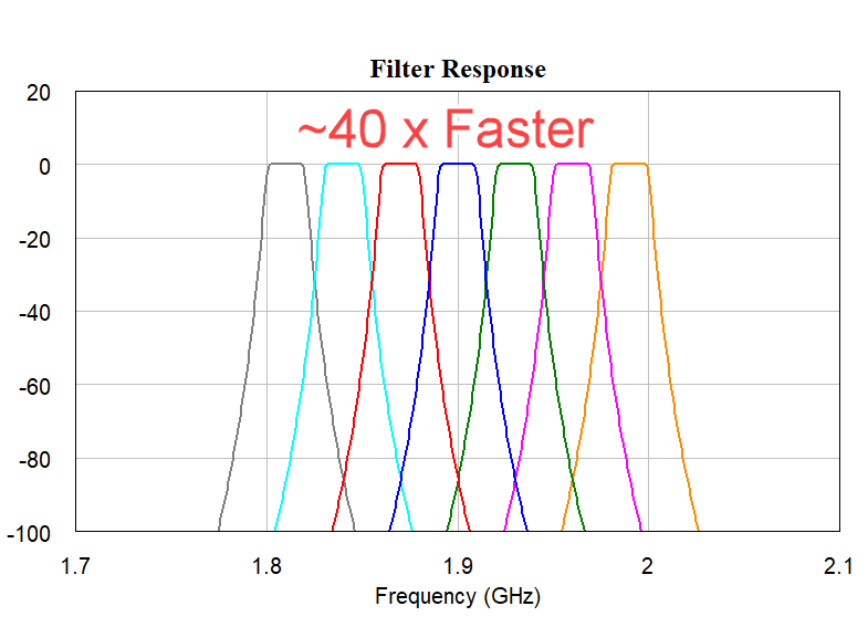
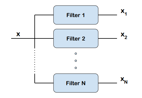
Simulate Multiple Module/Filter Test Benches Faster

Simulate many top-level test benches of extremely complicated modules in a fraction of the previous time.

Quickly simulate many bands to evaluate filter performance.

Intelligent reuse of underlying simulation data.

Average test cases ~40X faster.


Design and Analyze Filter Banks with Minimal Effort in VSS

Filter Bank

The project opens two system diagrams and respective graphs.

License Requirements: VSS Time Domain (VSS_250+)

  1. The Filter Bank system diagram shows a filter bank with 4 bandpass filters. The new RFSW_FRQ block is used to route the signals to the appropriate filter based on the signal frequency. Another RFSW_FRQ block is used after the filters to select the signal that corresponds to the appropriate filter and pass it to the output. The signal at the input of the filter bank is used to help the second RFSW_FRQ block identify the desired signal.
  2. The Filter Bank Response graph displays the measured frequency response of each filter, and also the combined response of the filter bank.
  3. A test bench is constructed to drive the filter bank with a modulated signal source, as shown in the "Modulated Test Bench" system diagram. The modulated signal frequency is switched and the output of the filter bank shows that it is tracking the signal frequency and selecting the appropriate filter internally.
  4. Spectra of the input and output signals display on the "Modulated Signals" graph.

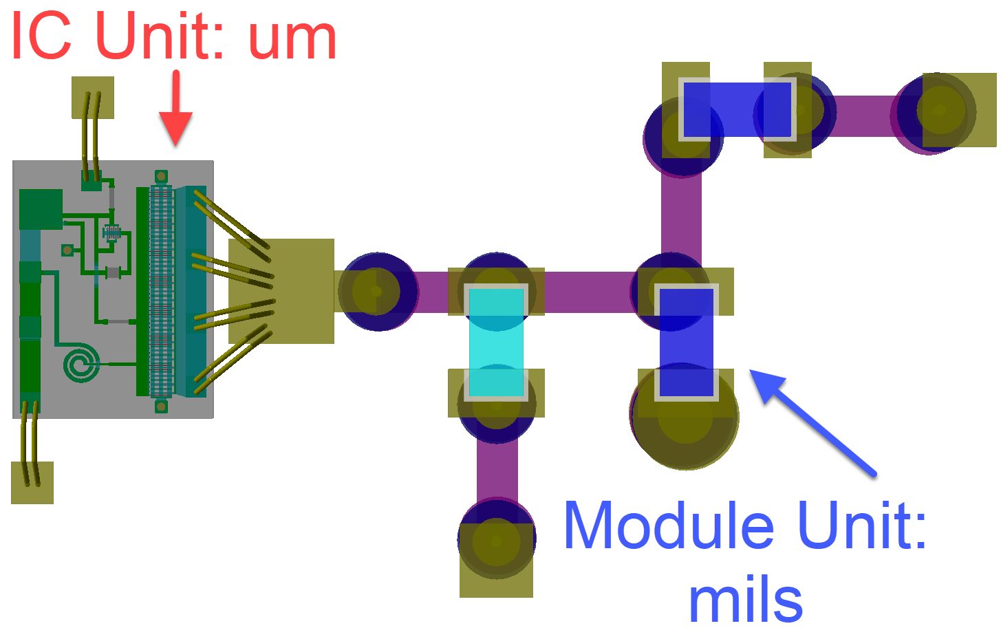
Design in your Unit of Choice for a Given Technology in Mixed-technology Designs

The project opens to two Schematic Views and their respective 2D Layout Views

License Requirements: Non-linear simulation and Layout (MWO_2X5+)

  1. In "1Stage_Amp" notice the units are in microns.
  2. In "Packaged_Amp" notice the units are in mils.
  3. Observe that "1Stage_Amp" is instantiated as a subcircuit in the "Packaged_Amp" schematic.
    • Technologies are mixed, yet designers can operate in the preferred unit for that technology.
  4. Open the AWR_MESFET layer process file.
    • Units can be set at an LPF level so designs using this technology operate in those units.
  5. Open the "Gain vs Output Power" graph.
  6. Right-click in the graph and choose Options to open the Rectangular Plot Options dialog box; click the Units tab.
    • Graphs can also honor technology so that performance metrics can be measured in the units of choice for a technology.
    • For example, MMIC designers may prefer GHz, while PCB/Module designers may prefer MHz.

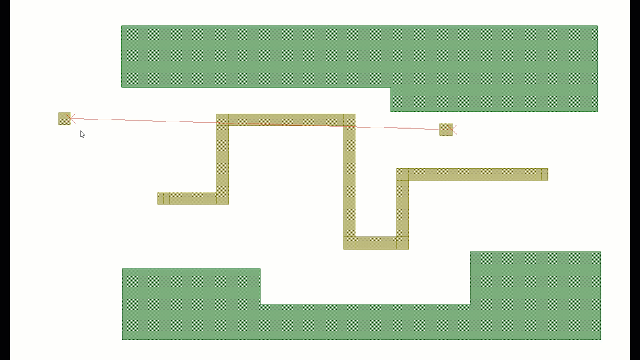
Navigate Dense Layouts while Obeying Metal-to-metal Separation Rules with Minimum Spacing Routing Guides

The project opens to a Schematic Layout View, sets the appropriate layout mode options, and loads the appropriate DRC rules for the Minimum Space Routing guides.

License Requirements: Layout (MWO_105+)

  1. Choose Layout > Layout Mode Properties to open the Layout Editor Mode Settings dialog box.
  2. In the Routing options section, verify that Minimum spacing guides, Reject clicks inside min spacing, Constrain to outside min spacing, and Disable self avoidance guides are selected.
  3. Choose Verify > Design Rule Check and look at the SEPARATION rules for each layer, then click Close.
  4. In the Schematic Layout double-click the ratline and begin routing from the left area pin. Route the trace to end on the right area pin by following the minimum spacing guides.
    • Try changing routing layers as you are routing by pressing Ctrl + Shift while scrolling the mouse wheel.
    • Note the difference in separation distances between the trace versus the ground plane shapes.
  5. Optionally, clear the check boxes you selected in step two. Leaving these options selected does not change behavior unless you have DRC rules loaded and are routing.