This page lists improvements to the AWR Design Environment for PA designers.
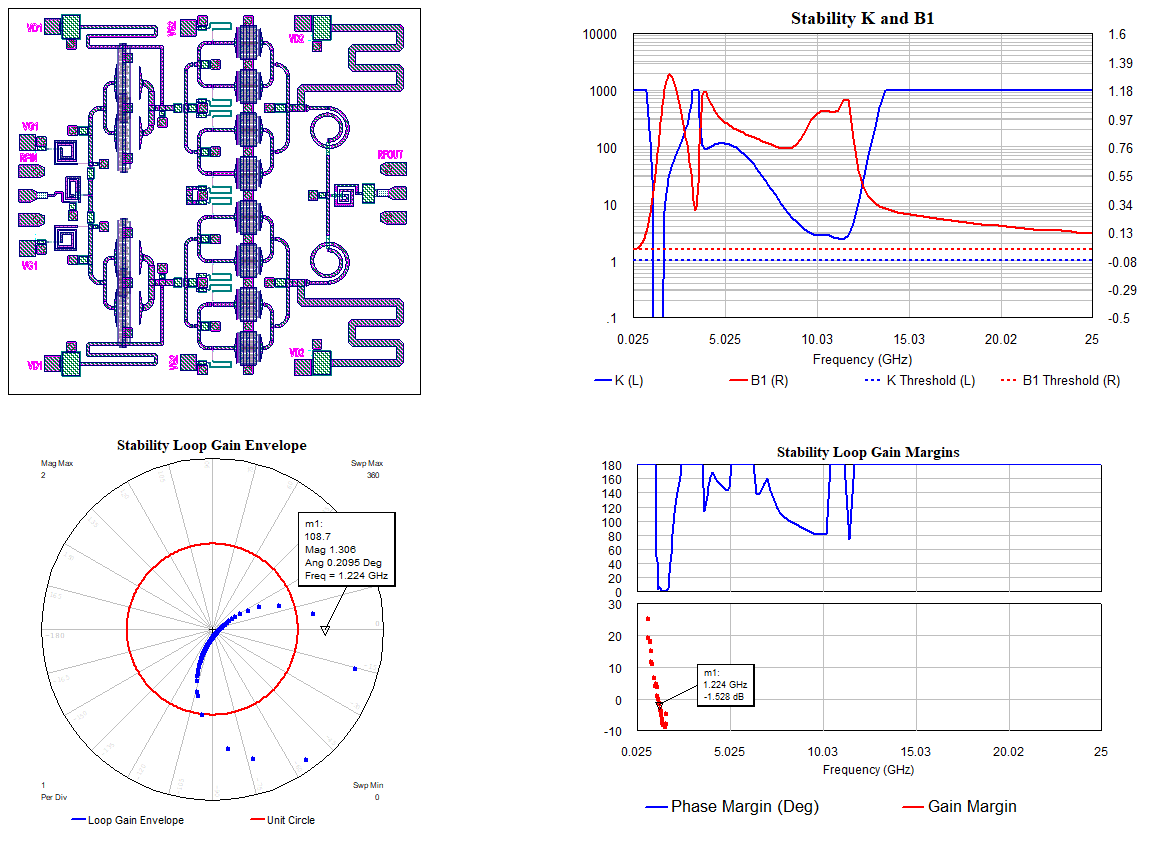
Perform Fast Linear and Nonlinear Stability Analysis Using Loop Gain Envelope Evaluation
The project opens to a data display page and simulates.
License Requirements: Linear or Nonlinear Simulation and Advanced Stability Analysis (STB_100)
In the Stability K and B1 Graph, note the K and B1 potential for instability. This is an easy to understand but not sufficient stability analysis metric.
In the Stability Loop Gain Margins Graph note the Gain Margins, some of which are negative, indicating instability.
Move the Marker and watch as the Loop Gain Envelope Graph changes. It is easily seen that as the Gain Margin becomes negative, the magnitude of the loop gain envelope is greater than one at zero degrees. This is a better indication of stabilty because it takes into account all possible termination impedances.
Open the optimizer by clicking Simulate > Optimize. There is an optimizer goal set up for 60 degrees of Phase Margin.
Start the optimization. In a short time, the phase margin envelope is optimized above the desired value and the instability is no longer present across the simulated frequency band and all possible termination impances.
The Stability Envelope series of measurements provide a much faster and still robust stability anslysis of your circuit. Rather than simulate N^2 reflection coefficients at each frequency, only N evaluations are needed.
The Phase Margin Envelope and Gain Margin Envelope measurements provide an easy to understand and directly optimizable metric for stabilty performance.
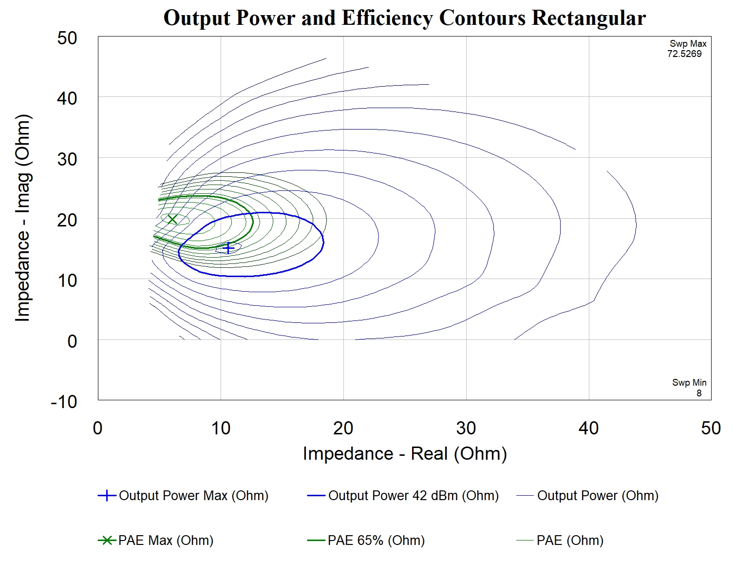
Directly Read Impedance Values from Load Pull Contours on Rectangular Real/Imaginary Graphs
The project opens to a data display page and simulates.
License Requirements: Load Pull (LPL_100)
Note the new Rectangular - Real/Imag graph type at the upper right side of the data display.
Contours shown on the Smith Chart and the Rectangular - Real/Imag graphs are the same.
This graph displays complex data, like load pull contours, on a Rectangular graph.
The axis can be set to gamma, impedance, or admittance.
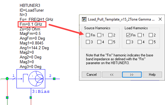
Simulate the Impact of Video Bandwidth or High-order Harmonic Impedance on PA Performance
The project opens to a load pull template schematic and a data display page and simulates.
License Requirements: Load Pull (LPL_100)
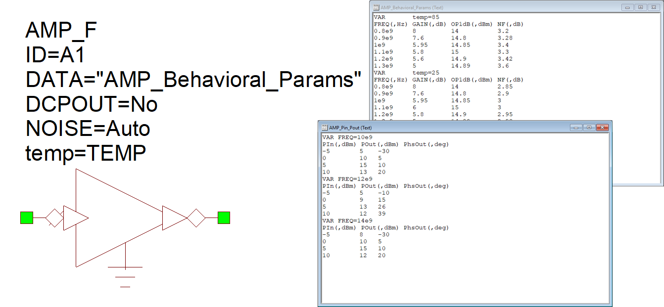
View the "Load_Pull_Template" schematic and note the new HBTUNER3 element that provides baseband impedance control for two-tone and modulated signal load pull and an unlimited number of harmonics.
Note the new Fm (and 4th/5th harmonic) options for load or source pull.
Click Cancel in the Load_Pull_Template Gamma Sweeps dialog box.
The contours in the data display show the high side/low side sensitivity to pre-simulated baseband impedance sweep.
Double-click the "Input Power vs. Index" graph to activate the view and drag the m1 marker up and down to change the input power.
Easily Set Up PA Model Reuse
This project illustrates improvements to the AMP_F file-based amplifier, which now supports two types of data files.
License Requirements: VSS Time Domain (VSS_250+)
AMP_F is updated to handle data files that were supported only by the NL_F block, which is now obsolete.
The first data format, used in the data file "AMP_Behavioral_Params", defines frequency-dependent behavioral
parameters (for example: gain, P1dB, NF, and IP3). The format can also include temperature dependency, which is implemented
by placing VAR temp=X at the beginning of each section of the file; this example includes three temperature settings.
The "Amp Model w Behavioral Params" system diagram uses the variable TEMP to define the simulation temperature
and is swept using the SWPVAR block. A range of frequencies is defined in the system diagram options dialog box
on the RF Frequencies tab. The Gain and Noise Figure are measured using the RFB simulation and are
plotted in the "Behavioral Params Gain" and "Behavioral Params NF" graphs.
The second data format, used in the "AMP_Pin_Pout" data file, defines the power-in power-out relationship
(the AM/AM and AM/PM characteristics of a device). This format can also account for frequency dependency, which is
achieved by placing VAR FREQ = Y before each AM/AM/PM data set. This example illustrates a device specified by its
AM/AM/PM characteristics over three frequencies. The "Amp Model w Pin Pout Model" system diagram illustrates a different
method of characterizing the device by using a VNA to sweep the power and frequency of the source and measure the
device response. The AM-to-AM characteristic of the device is plotted in the "Pin Pout AM to AM" graph using both
RFB and Time Domain measurements. AM-to-AM curves are plotted for various frequencies, as defined in the VNA.
See the AMP_F Help and the VSS Getting Started Guide for more information.
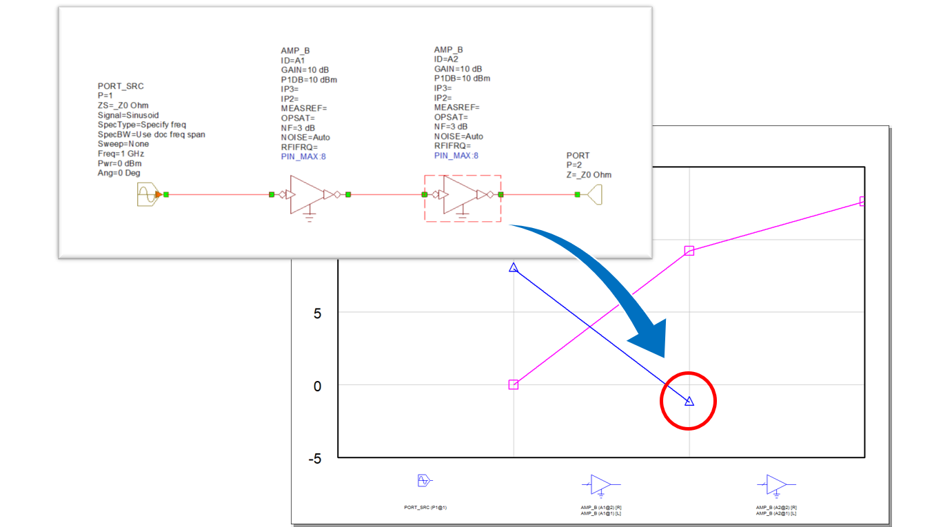
Inspect System Diagrams for Damage from Overdriving the Devices
This project shows how to use the new cascaded damage indicator measurement, C_DAMAGE, in VSS.
License Requirements: VSS RF Budget (VSS_150+)
C_DAMAGE computes cascaded operating point headroom relative to a power level at which damage is considered
to occur at block input ports using the VSS RF Budget Analysis simulator. C_DAMAGE is similar to C_HDRM except
that instead of comparing the input power to the 1 dB compression point, it is compared against a threshold
above which damage is considered to occur, referred to as PIN_MAX. Such values are specified for individual
blocks by adding a user attribute named PIN_MAX.
You can add a UATTR annotation to the system diagram (from the Annotate > Attributes folder) to
highlight the block(s) operating at input levels exceeding their respective PIN_MAX settings.
This example project consists of a cascade of two PAs driven with a PORT_SRC at 0 dBm. The PIN_MAX attribute
is set to 8 dBm for both PAs in the cascade. The second PA is highlighted to show that it is operating above
its defined PIN_MAX setting, and the simulation results show that it is driven approximately 1.2 dB beyond that level.
See the AWR Microwave Office Measurement Help for more information.
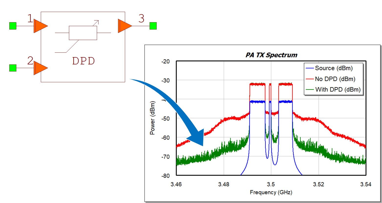
Evaluate Device Linearization before Building it / Test Drive Classic or Commercial DPD Algorithms
This example illustrates linearization of a PA using the new DPD block in VSS.
License Requirements: VSS Time Domain (VSS_250+)
The new DPD block offers several classic Digital Pre-Distortion algorithms such as Memory Polynomials and
Generalized Memory Polynomials.
This example shows an OFDM signal at 3.5 GHz configured to simulate a multi-user type operation. The signal
is fed to a driver amp and then into a power amplifier implemented as a circuit schematic in Microwave Office.
The DPD uses a feedback signal from the device output which, along with the source signal, is used for
initial calculations of the selected algorithm and then for incremental updates. The block offers various
solvers that can be used for the initial DPD setup.
Results compare device performance with and without the DPD, showing improvements in spectral regrowth,
IQ constellation distortion, and CCDF.
Options for commercial DPD solutions are available, allowing you to run the same algorithms in
simulations as in the lab.
See the VSS System Block Help for more information.