This page lists improvements to the AWR Design Environment for module designers.
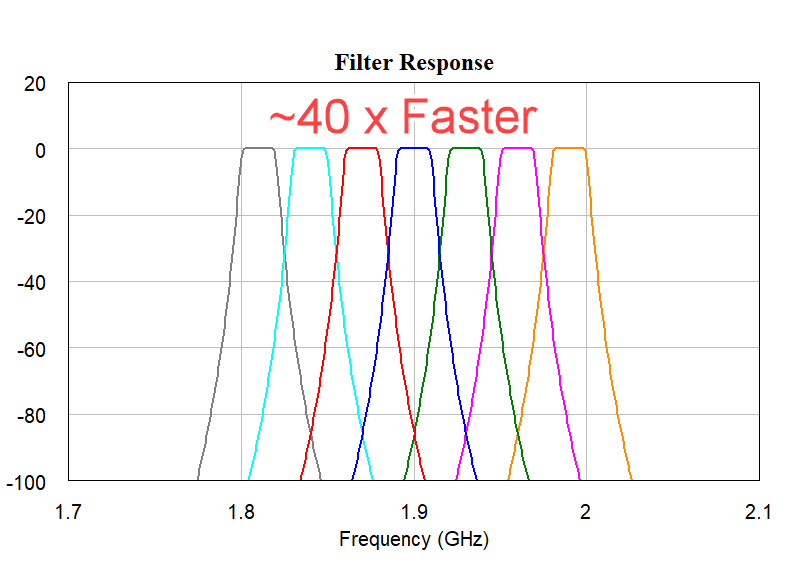
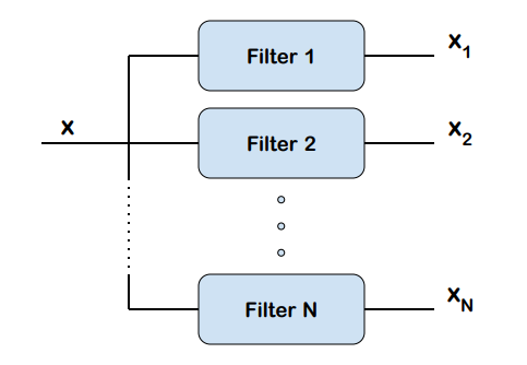
Simulate Multiple Module/Filter Test Benches FasterSimulate many top-level test benches of extremely complicated modules in a fraction of the previous time. Quickly simulate many bands to evaluate filter performance. Intelligent reuse of underlying simulation data. Average test cases ~40X faster. |
|
|
|
|
Design and Analyze Filter Banks with Minimal Effort in VSSFilter BankThe project opens two system diagrams and respective graphs. License Requirements: VSS Time Domain (VSS_250+)
|
|
|
|
|
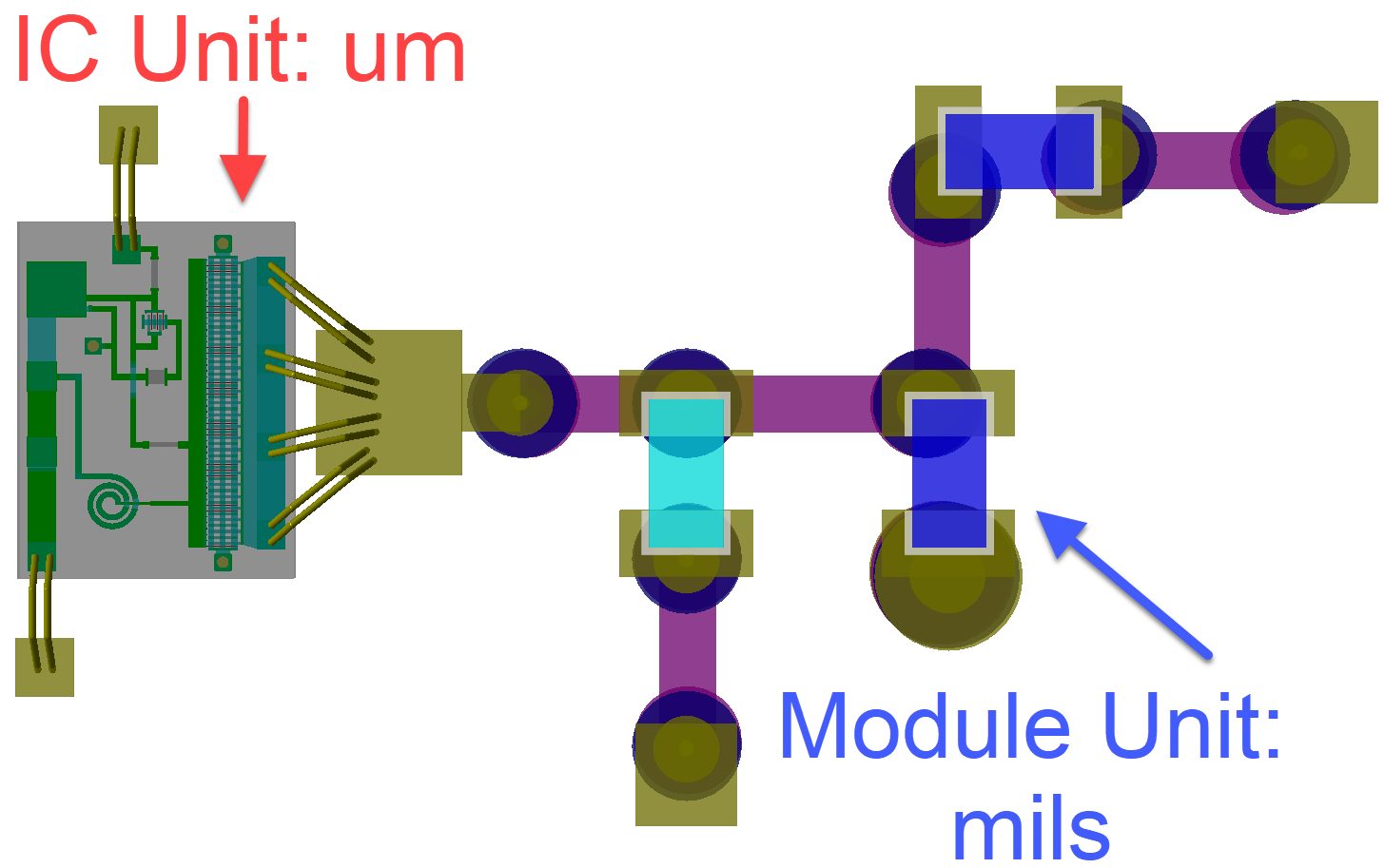
Design in your Unit of Choice for a Given Technology in Mixed-technology DesignsThe project opens to two Schematic Views and their respective 2D Layout Views License Requirements: Non-linear simulation and Layout (MWO_2X5+)
|
|
|
|
|
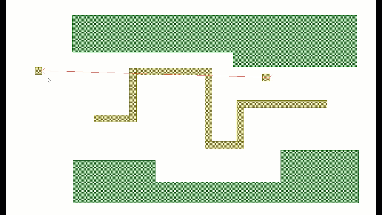
Navigate Dense Layouts while Obeying Metal-to-metal Separation Rules with Minimum Spacing Routing GuidesThe project opens to a Schematic Layout View, sets the appropriate layout mode options, and loads the appropriate DRC rules for the Minimum Space Routing guides. License Requirements: Layout (MWO_105+)
|
|
This page contains improvements to the AWR Design Environment for module designers.
License requirements: Layout with iNets (MWO-XX6+)
Leverage the power of AXIEM in the Cadence Virtuoso RF Solution.
|
|
|
|
|
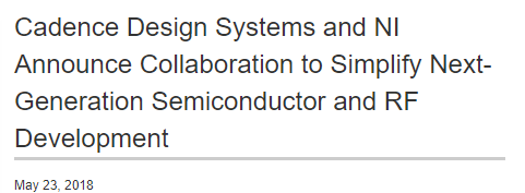
Easily modify existing iNet routes using the Reshape Route command.Reshape RouteThe project will open to an iNet routed too close to a via.
|
|
|
|
|
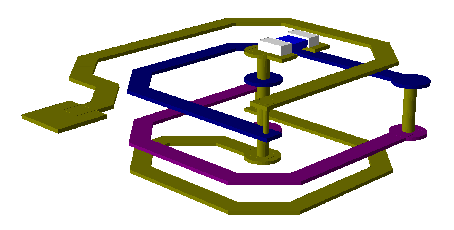
Route iNet bends with new bend styles.Chamfered and rounded bend stylesThe project will open to a Schematic Layout with an iNet spiral module inductor
|
|
|
|
|
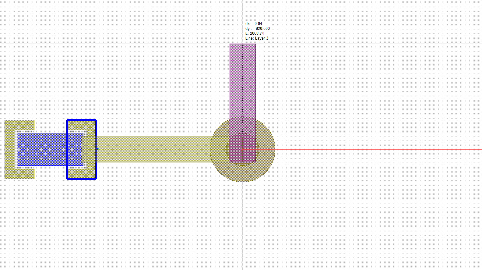
Change iNet via types on the fly.Change iNet vias with hot keyThe project will open to a Schematic Layout with an un-routed iNet (ratline)
|
|
|
|
|
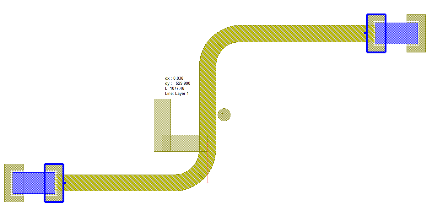
Manually move iNet vias.Move iNet viasThe project will open to a Schematic Layout with an iNet and vias in their default locations.
|
|
|
|
|
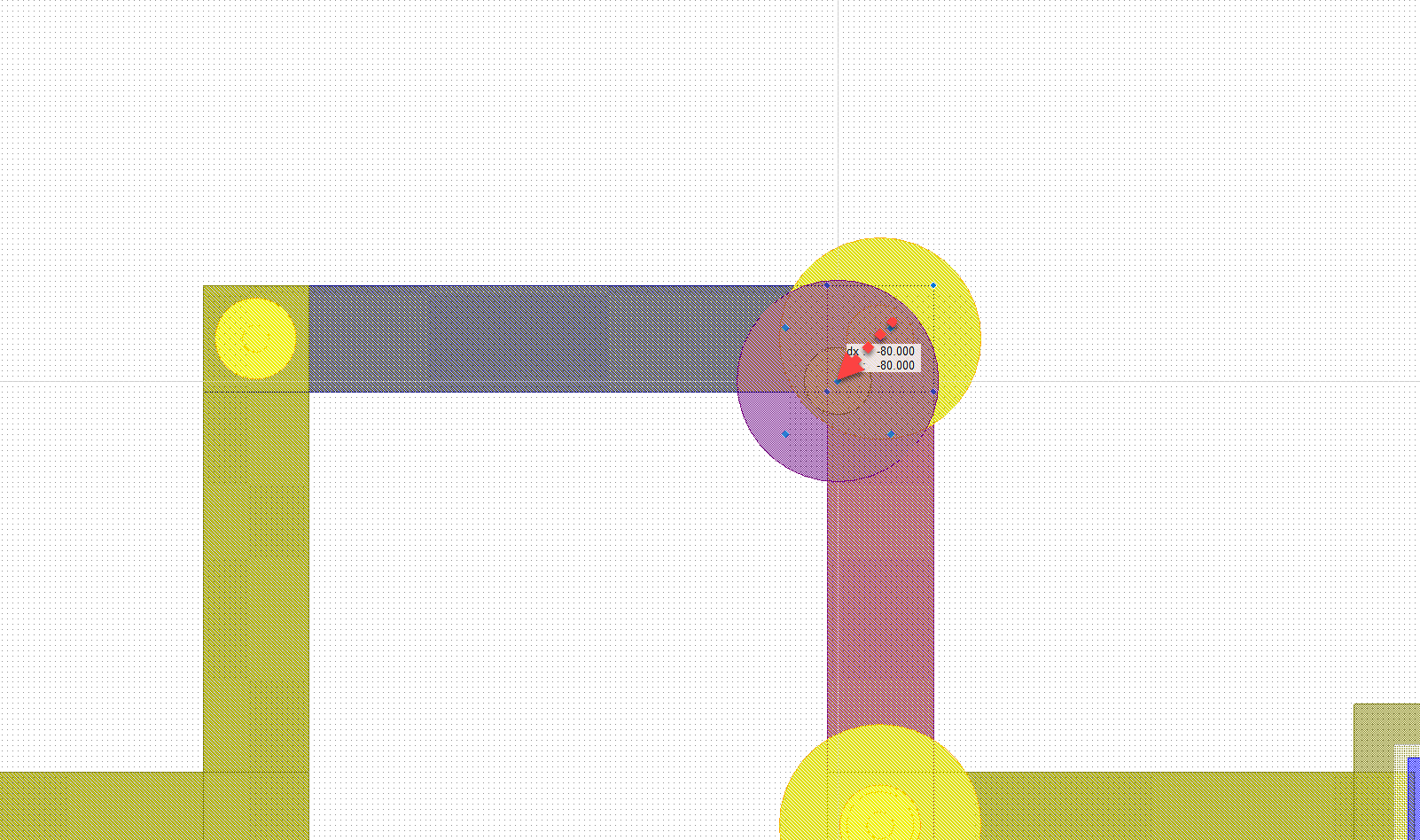
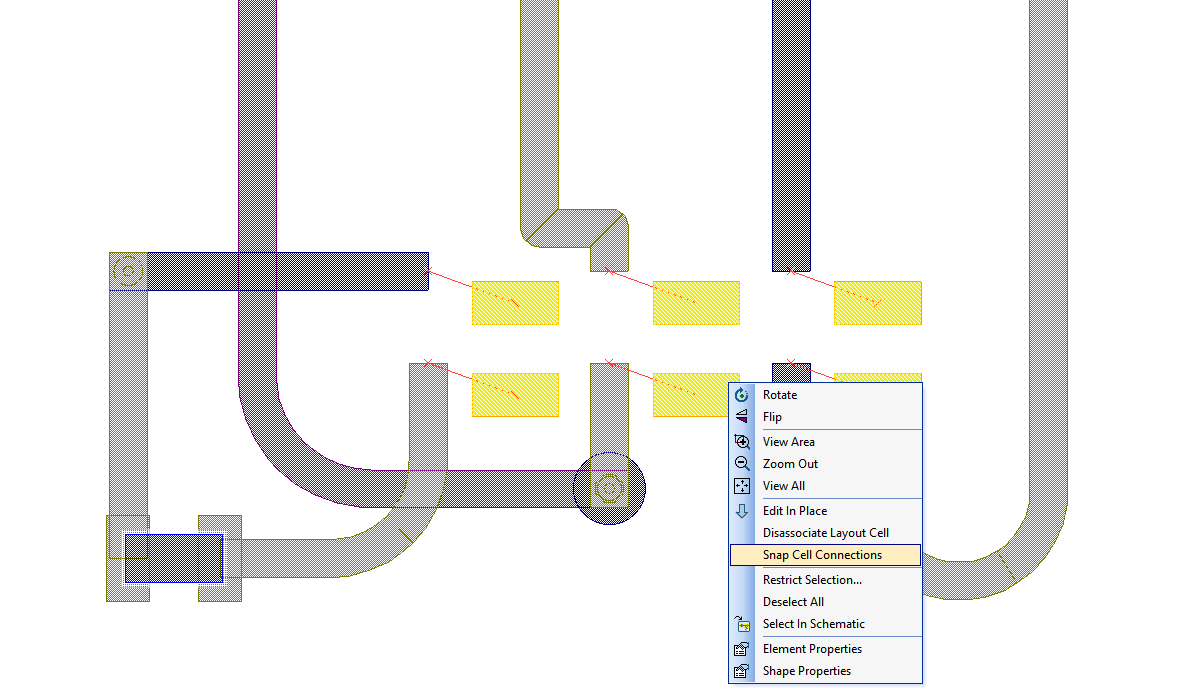
Auto-reconnect disconnected iNet routes.Snap cell connectionsThe project will open to a Schematic Layout with several iNet routes connected to all six pins of an SMD footprint.
|
|
|
|
|
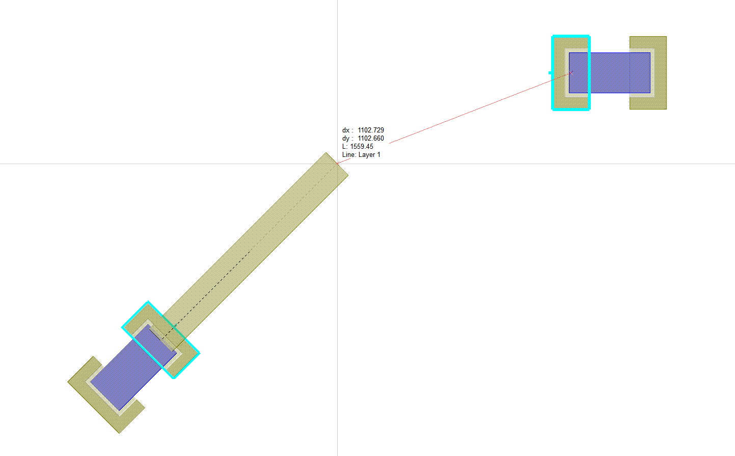
Start iNet routes orthogonal to any pin.Orthogonal startThe project will open to a Schematic Layout with an un-routed iNet (ratline) with one of the cells rotated 45 degrees.
|
|
This page contains improvements to the AWR Design Environment for module designers.
Easily Manage complex multi-technology designs (PCB, IC, LTCC, etc.).Manage Multiple TechnologiesThis demo will show the improvements made to the framework to support multiple technologies in a single project.
|
|
|
|
|
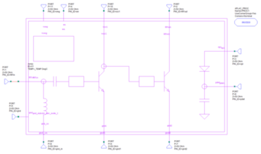
Validate designs created by users in different tools by co-simulating with Cadence Virtuoso designs.Cadence Spectre Co-simulationThe project will open to a Schematic and Graph window and simulate. License requirements: Translated Spectre Designs (SPS-100), Nonlinear simulator (MWO-2XX), and VSS Communication standards (VSS-350)
|
|