This page lists new capabilities in the AWR Design Environment for phased array designers.
License Requirements: VSS Time Domain and the 5G or Radar Library (VSS_250+, W5G_100 or RDR_100)
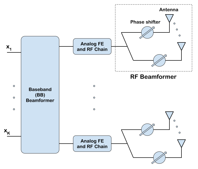
Efficiently Design, Configure and Simulate Phased Array SystemsUse Buses to Simplify Implementation of Various Phased Array ArchitecturesExamples include Digital or Hybrid Beamformers |
|
|
|
|
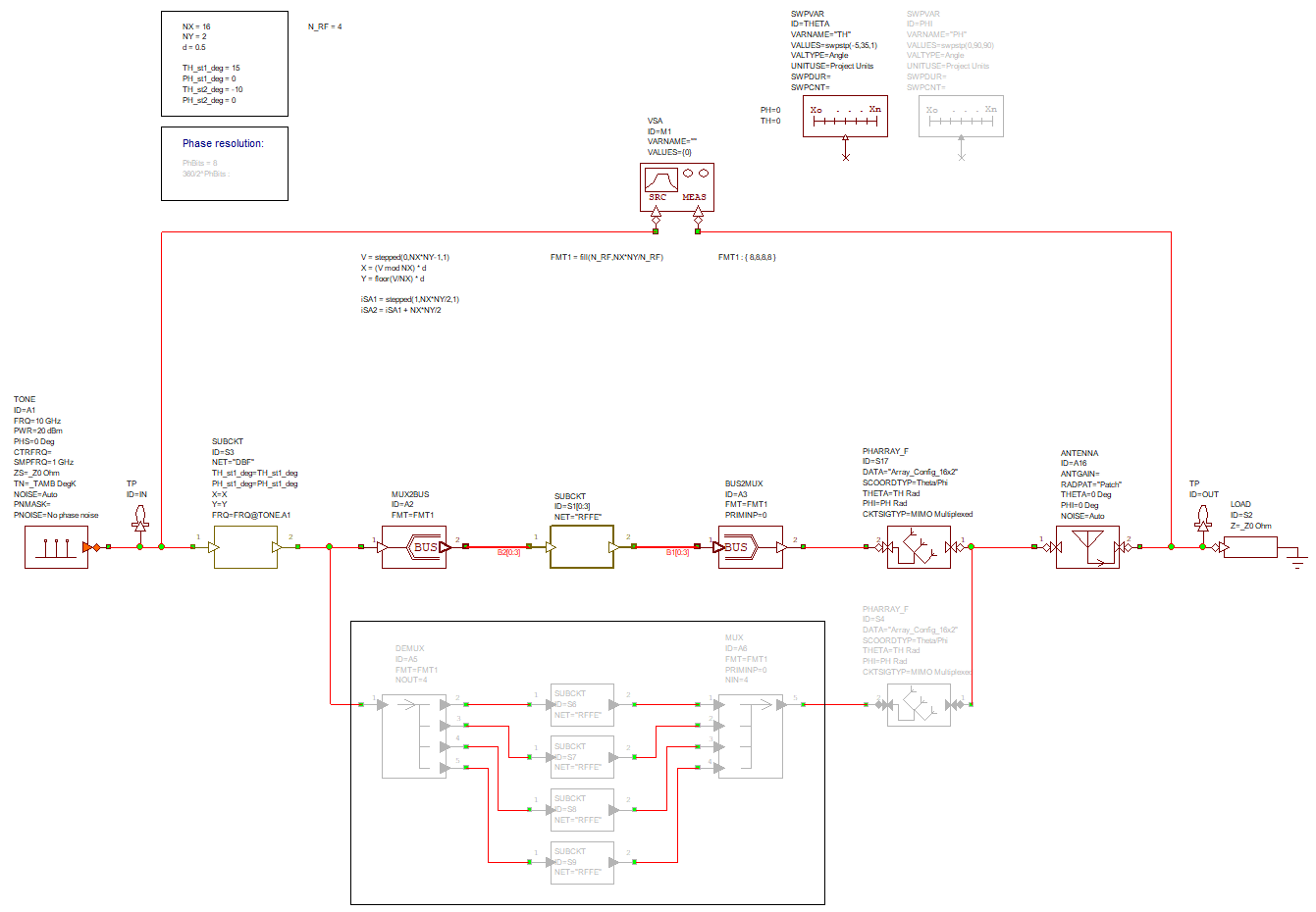
Hybrid Beamforming ExampleThe project shows a partially-connected hybrid beamforming architecture, illustrated in the figure on the right.
|
|
|
|
|
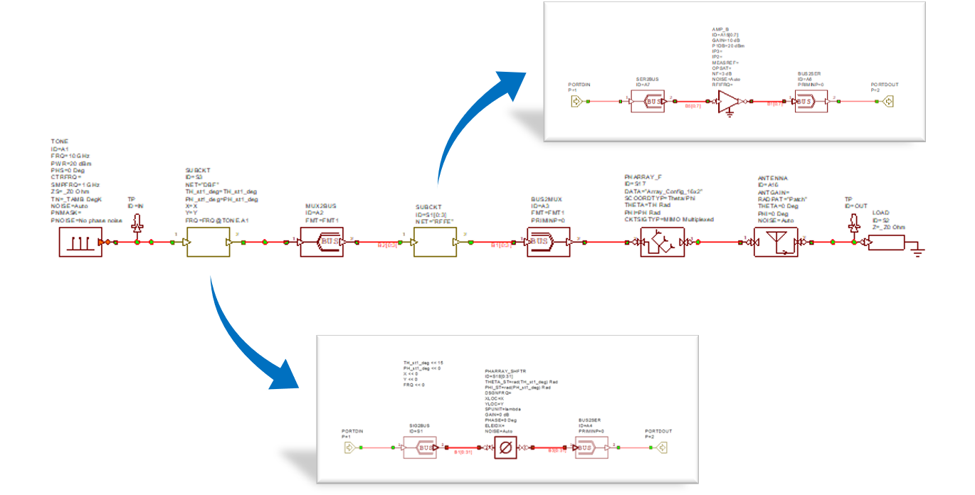
Hybrid Beamformer Design
|
|
|
|
|
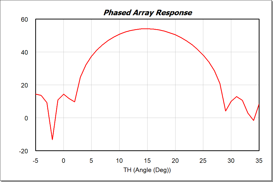
Phased Array ResponseThe array response is measured over a range of angles and shown in the graph on the right. This project uses the VSS Time Domain simulator for this measurement. The measurement results are stored in the project and displayed in the "Phased Array Response" graph. Note that running the simulation takes several minutes to generate the full array response. |
|
This page contains improvements to the AWR Design Environment for phased-array designers.
License Requirements: VSS-250 or greater and either the 5G library (W5G-100) or the Radar Library (RDR-100)
Efficiently design, configure and simulate phased array systemsPerform trade-offs between various phased array design options:
Generate full system-level designs of the phased array systems that can be used for further analysis, can be incorporated into larger systems to create more complex architectures.Generate schematic and EM layouts of the phased array for further analysis with circuit and/or EM simulators in AWRDE. |

|
|
|
|
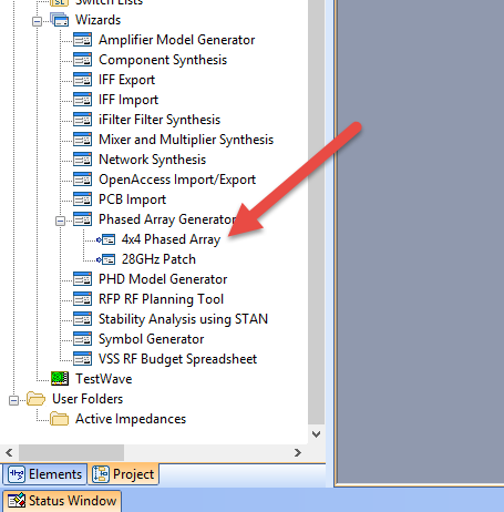
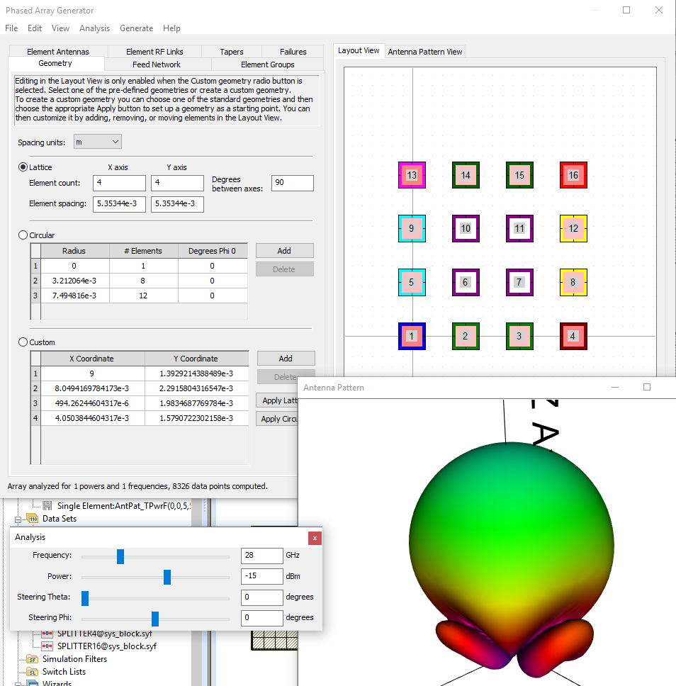
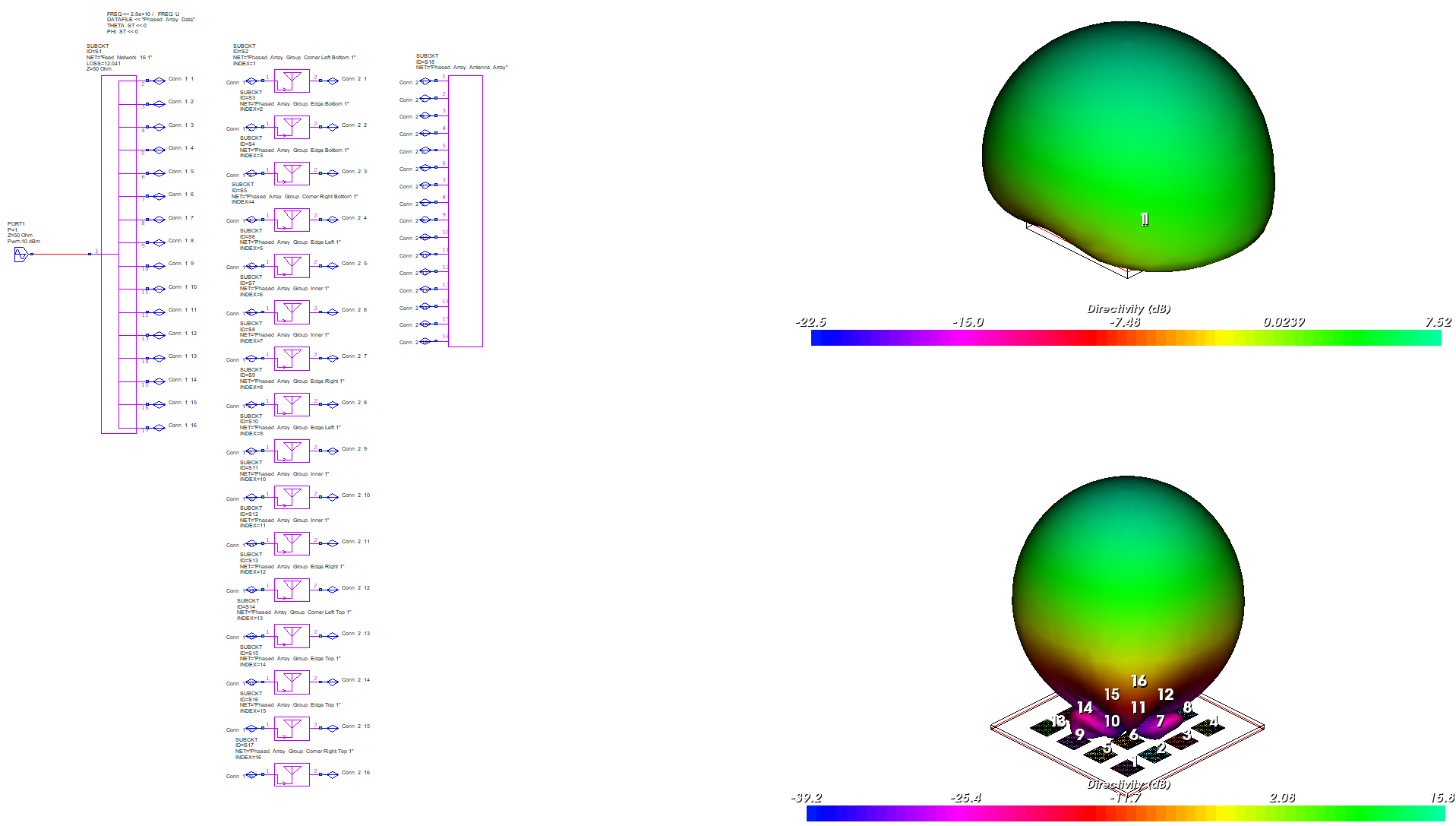
Phased Array GeneratorThe project contains a pre-configured phased array design to simplify the configuration process. Start by clicking the Open Project button below, which will open the example project. Under the Wizards node in the Project tab, locate the Phased Array Generator Wizard and double-click on the 4x4 Phased Array instance. This will open the Phased Array Generator wizard with the pre-configured phased array. |
|
|
|
|
Array Design Trade-offsUse this wizard to define the array configuration of your choice. From the menu bar, click Analysis/New Floating Antenna Pattern View to see a 3D response of the phased array and immediately observe the effect of various configuration choices. Select the available tabs in the wizard and explore / play with the following characteristics of the array:
When finished with configuration of the phased array, close the wizard and save or discard changes. |
|
|
|
|
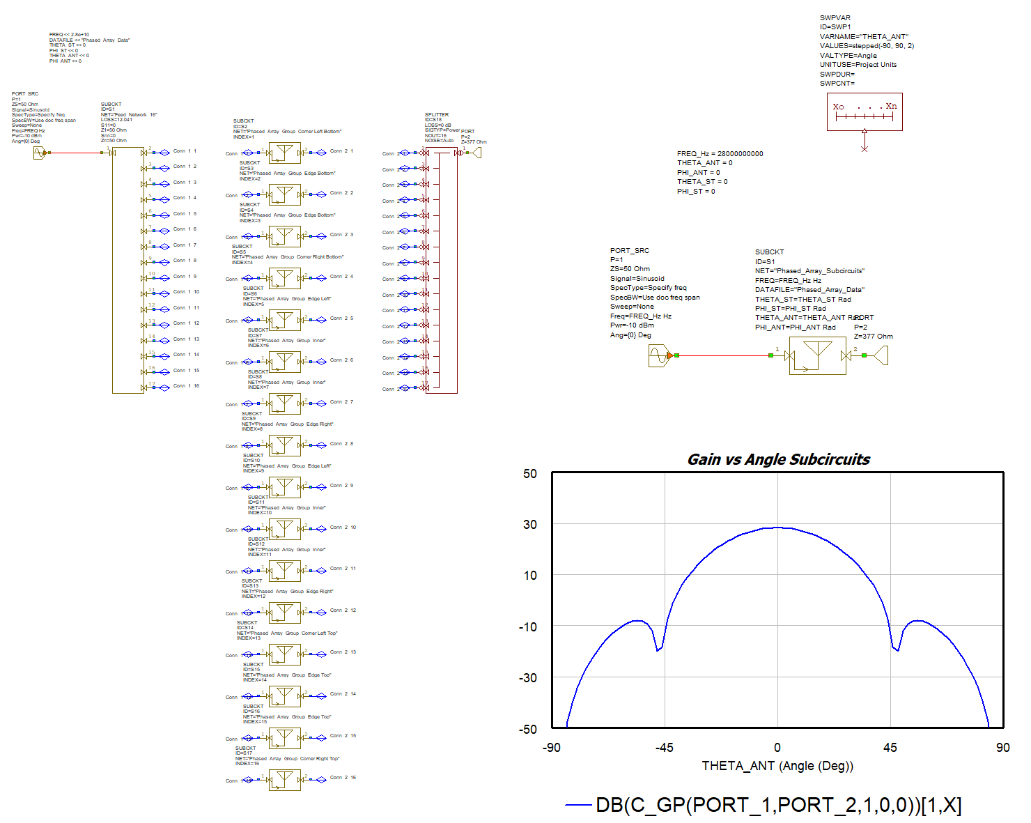
Generate System Diagrams and TestbenchOnce content with the array configuration, click Generate > Generate System Diagrams... An implementation of the phased array as a series of subcircuits will be generated. All subcircuits are automatically configured with the correct phase shifts and taper values. A testbench and a response graph are also created. This array implementation may be used for further analysis in VSS or as part of a larger system. To view a pre-generated testbench, system diagrams and array response click the button below. |
|
|
|
|
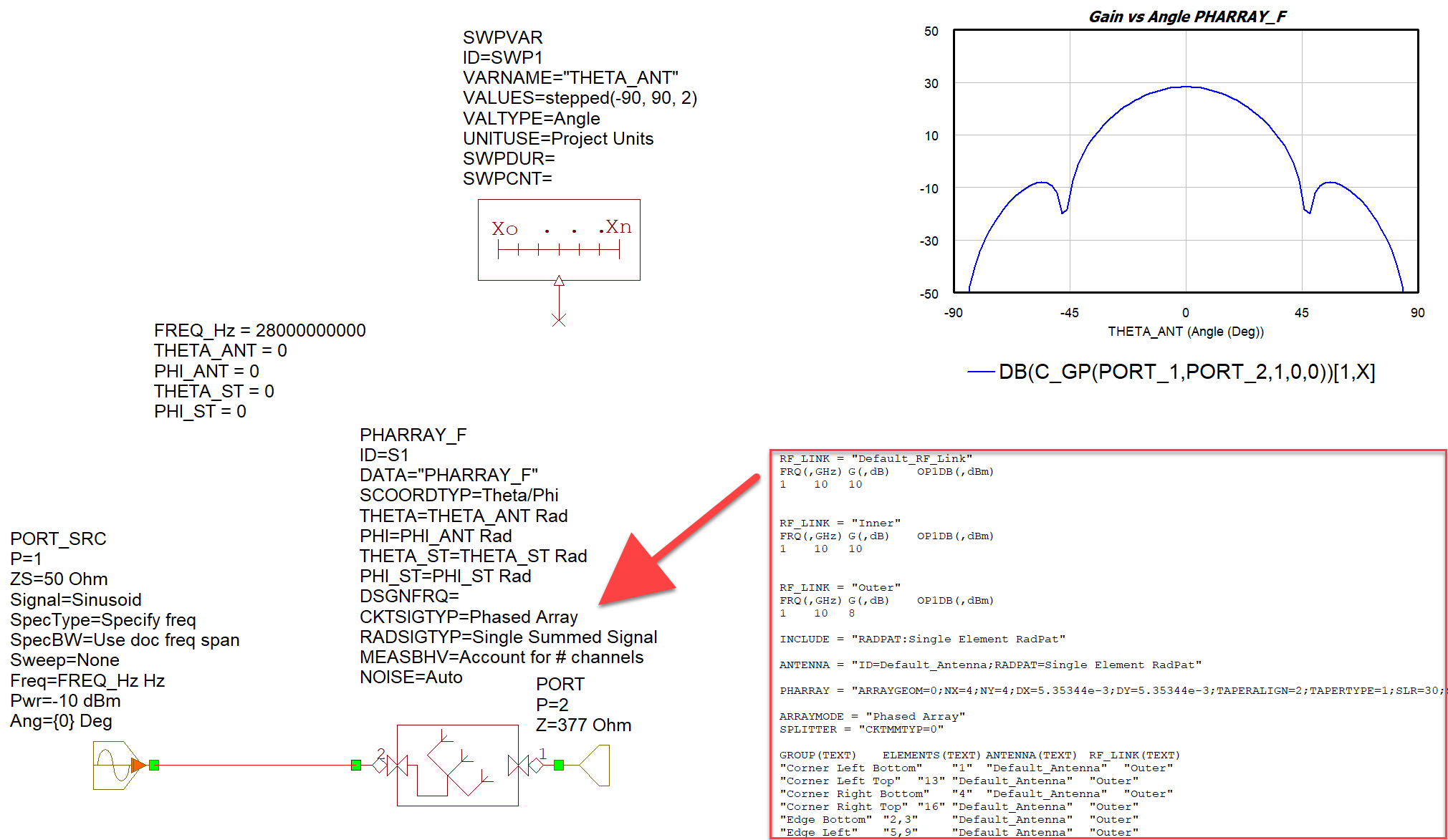
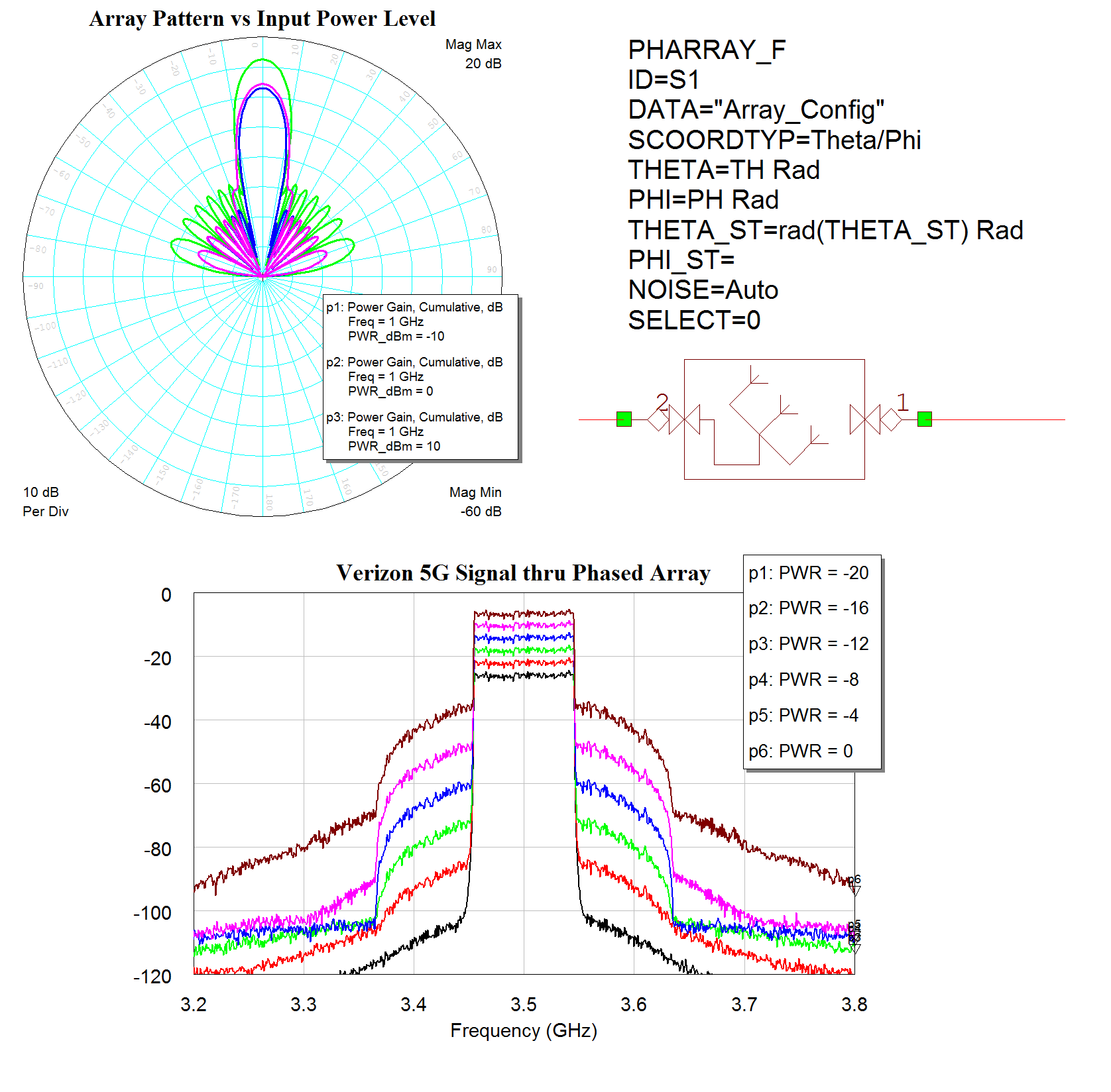
Generate PHARRAY_F Data File and TestbenchA PHARRAY_F block may be used to model the designed phased array in VSS. To generate the configuration file for PHARRAY_F, click on Generate > Generate PHARRAY_F Data File... A testbench containing the properly configured PHAARRAY_F, the configuration file and a response graph are created. The configuration file may be appended with additional configuration options, such as mutual coupling, etc. Similarly, this array implementation may be used for more detailed analysis in VSS or as part of a larger system. To view a pre-generated testbench, configuration file and array response click the button below. |
|
|
|
|
Generate Schematic and EM LayoutThe wizard may also create a schematic of the phased array system and an EM layout of the phased array, which can be used for a wide range of purposes. If a patch is already designed and included in the project, the wizard can use it during the generation process. One of the usages of the created schematic may be to measure the active impedances at each of the antenna element ports as a function of the scan angle. The EM layout may be also used to perform in-situ analysis and calculate the response of the phased array using EM simulations. To view pre-generated schematics, 3D layouts and radiation patterns click the button below. |
|
This page contains improvements to the AWR Design Environment for phased-array designers.
License Requirements: VSS-250 or greater and the 5G library (W5G-100) or the Radar Library (RDR-100)
Efficiently simulate extremely large phased arrays.Design 5G MIMO systems, including RF and beamforming architectures.Discover the impact of phased arrays on overall system performance.Utilize yield analysis or optimization tools to evaluate and improve designs. |
 |
|
|
|
Phased Array EnhancementsOpens the Phased Array (PHARRAY_F) example, tiles out the main graphs and simulates. All of the phased array enhancements are shown in this view, but they can be displayed individually using the demo buttons below. |
|
|
|
|
ResponseThis demo illustrates using the PHARRAY_F model to evaluate the response of a phased array while taking into account radiation patterns and RF links of each element.
|
 |
|
|
|
Modulated SignalsThis demo illustrates passing modulated signals through the PHARRAY_F model.
|
 |
|
|
|
YieldThis demo illustrates the impact of gain and phase variation on the array antenna pattern.
|
 |