Go to playground home.

Schematic

This page lists improvements to the Circuit Schematic and System Diagram editors in the AWR Design Environment.


V15


Further Customize Schematic Appearance with Filled Symbols


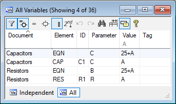
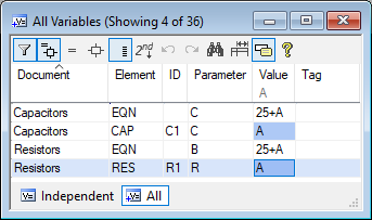
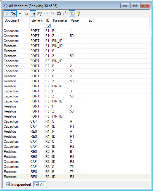
Manage Design Data with Variable Browser Improvements

The project opens to two schematics, a Global Definitions page, the Variable Browser, and then simulates.

  1. Each of the schematics depend on both Global and Local variables.
  2. The Variable Browser is currently showing a V11+ view that contains filterable lists of all the independent variables and supports group editing, tuning control, optimization control, and other functions.
  3. Click the All button at the bottom of the Variable Browser.
  4. The All view displays all variables (both independent and dependent) and is intended to help manage projects.
  5. At the top of the Variable Browser are controls for the following (hover the cursor over the buttons for balloon Help):
    • Show elements, equations, or both.
    • Show all element parameters or just the ID.
    • Show/hide secondary parameters.
  6. To see the project management power of this variable view, enable the controls for Show elements and equations and Show all parameters. Enter A as a filter, just below the Value column heading.
  7. Note that the A variable is used directly in two schematics and in two equations in schematics.
  8. Select the Value column for the "CAP" row, then multi-select (Ctrl + Click) the Value column for the "RES" row.
  9. Change one of the selected A values to D and press Enter.
  10. Both elements are updated to use the D Global Definition. Optionally simulate (F8) to see the difference.
  11. Click the Undo button in the Variable Browser to change both elements back to the A value and then click the Redo button in the Variable Browser to switch both elements back to the D value.
  12. Click on the entries in the Element column to zoom to the corresponding element or equation.
  13. With the Variable Browser improvements, design management, including changing many elements or equations at once with the Undo/Redo capability are supported.

V14


This page contains improvements to the Circuit Schematic and System Diagram editors in the AWR Design Environment.

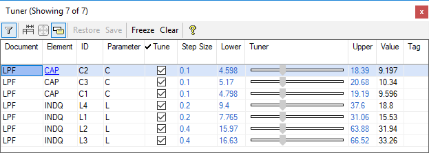
Tune on an unlimited number of variables in an amazingly compact, yet readable dialog.

New Tuner

The demo opens the lpf_lumped example, simulates, and opens the tuner.

  1. Tune on any of the variables.
    • Click and drag on the slider for the variable you want to tune on.
    • Select the slider and use the arrow keys to move one step at a time.
  2. Filter on any column by typing in the text area under each column header.
    • Note that hovering over the toolbar buttons pops up balloon help with descriptions about the button function.
    • Make sure filtering is enabled by clicking the Filter toolbar button
  3. Click on any entry in the Element column to show the Circuit Schematic and Element being tuned.

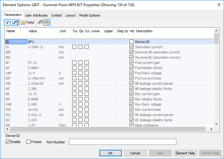
Filter, group edit, and spend less time changing tabs in the new element parameters dialog

New Element Parameter Dialog

This demo opens the nonlinear_example project, opens the IV_Curve Circuit Schematic, and opens the element properties for the transistor.

  1. Note that hovering over the toolbar buttons pops up balloon help with descriptions about the button function.
  2. Enable the secondary parameters by clicking the 2nd toolbar button.
  3. Filter on a parameter name by type in the Name column.
  4. Sort parameters by clicking any of the column headers.
  5. Multi-select by holding CTRL and selecting multiple parameters.
    • This is useful for enabling tuning or optimization on sets of variables.
  6. Show yield settings by clicking the yield toolbar button.
  7. Auto-size column widths by pressing the auto-size toolbar button.

Customize your schematics' appearance with infinite symbol colors

Easily identify schematic elements without zooming in.


Quickly and easily create complex System Diagrams with Buses

VSS Bus Support

This demo opens the project, displays the proper System Diagrams and Graphs, and then simulates.

  1. Note that the Reference System Diagram shows a 4 channel Phased Array simulation wired the traditional way.
  2. Note that the Array with BUS models System Diagram shows the same 4 channel Phased Array simulation wired with buses and vector instances and is significantly more simple.
  3. Note that the both tables show the same answer which illustrates that both System Diagrams are electrically equivalent.
  4. Further details can be found in the Design Notes in the project.

V13


This page contains improvements to the schematic editor in the AWR Design Environment.

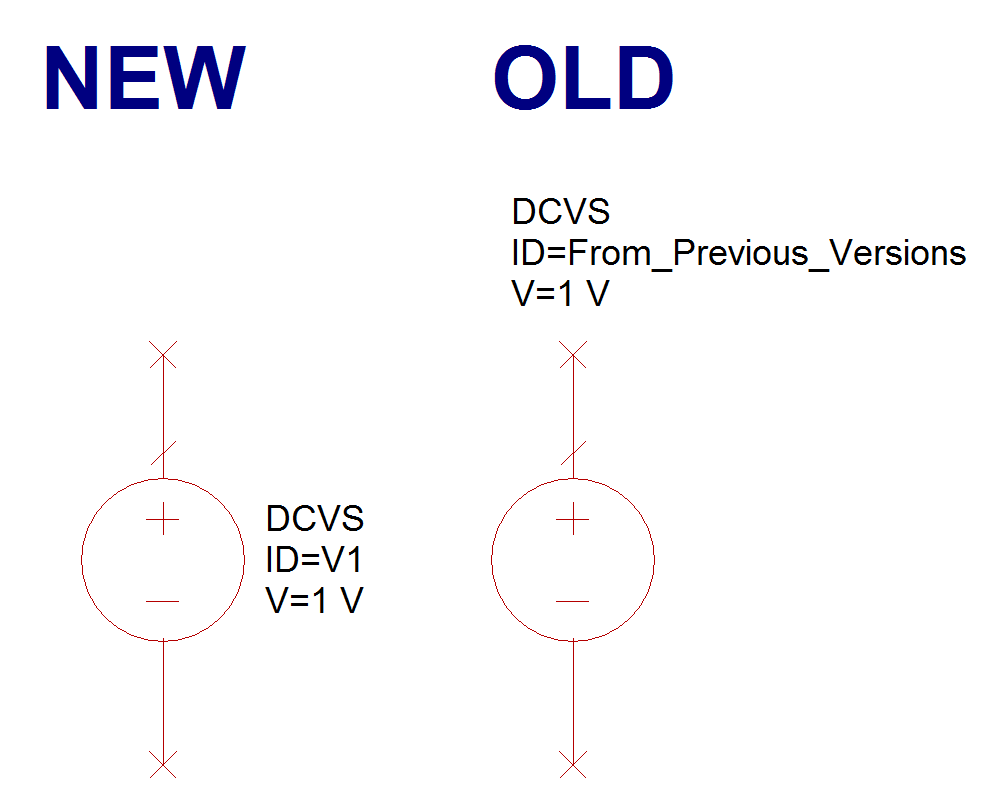
Parameter frames for vertically-placed 2-port elements are now on the right instead of above the element.

No Longer Need to Move Parameter Frames After Placing Vertical Elements

The demo creates a new project, opens a Schematic that contains a DCVS placed in v12, and puts a new DCVS in placement mode.

  1. A DCVS source is ready to go in "placement mode" (e.g. as if it had been dragged in from the Elements list).
  2. Click anywhere to place the element.
  3. Notice the parameter frame in the new DCVS places to the right of the element instead of above it.

Reduce time-wasting errors by wiring S-parameter blocks using node names rather than node numbers.

Touchstone (s-parameter) Files With Name Based Connectivity

The demo opens the project to a schematic to show two touchstone subcircuits; one with port names and one without.