This page contains improvements to the AWR Design Environment for PCB designers.
License requirements: Layout and EMSight™, AXIEM, or Analyst
Use best-in-class EM simulators to verify your PCB designs by importing them with ease for all PCB design tools.Quickly and easily prepare designs for EM analysis with new layout tools and selection capabilities. |
 |
|
|
|
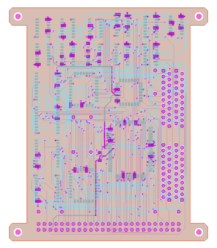
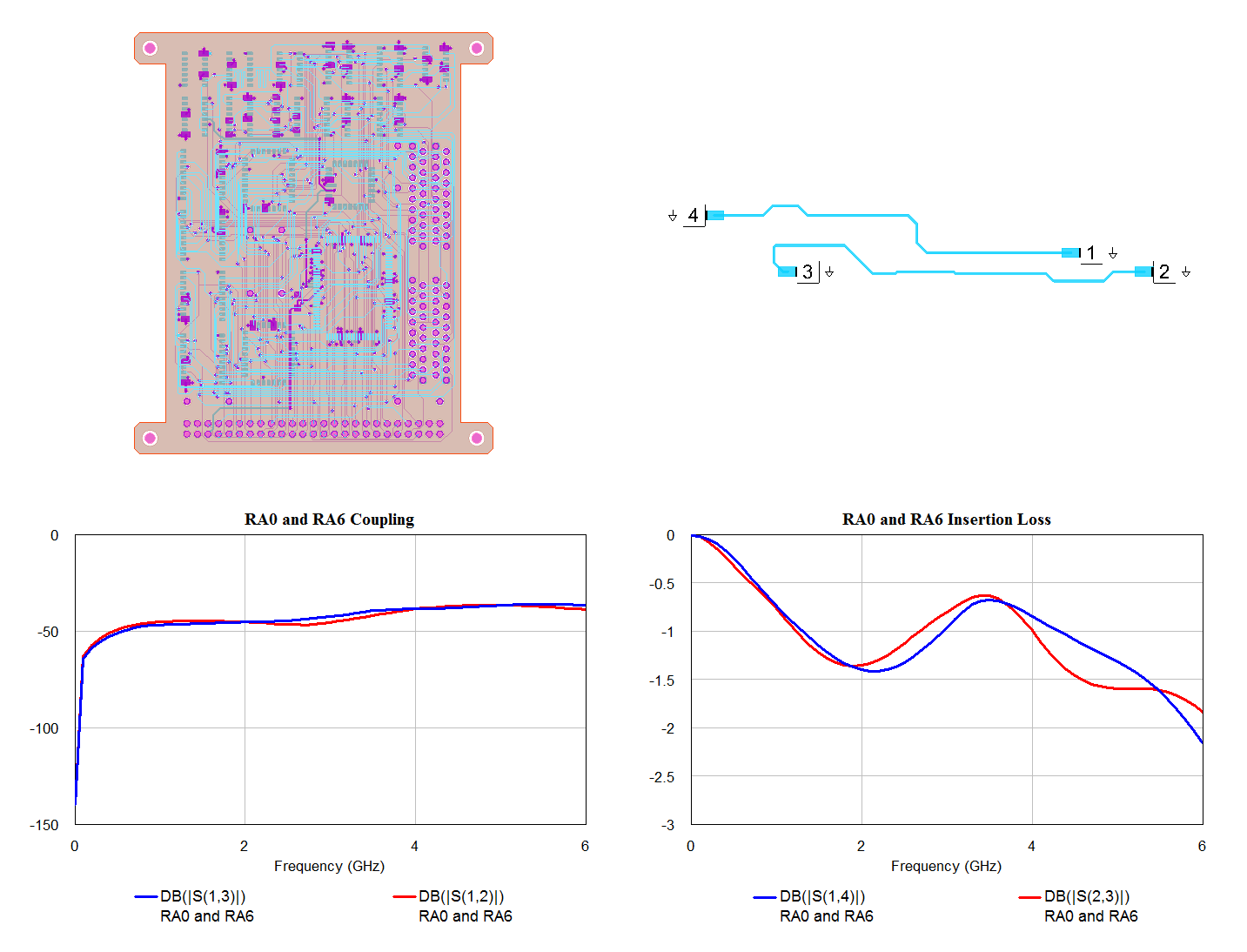
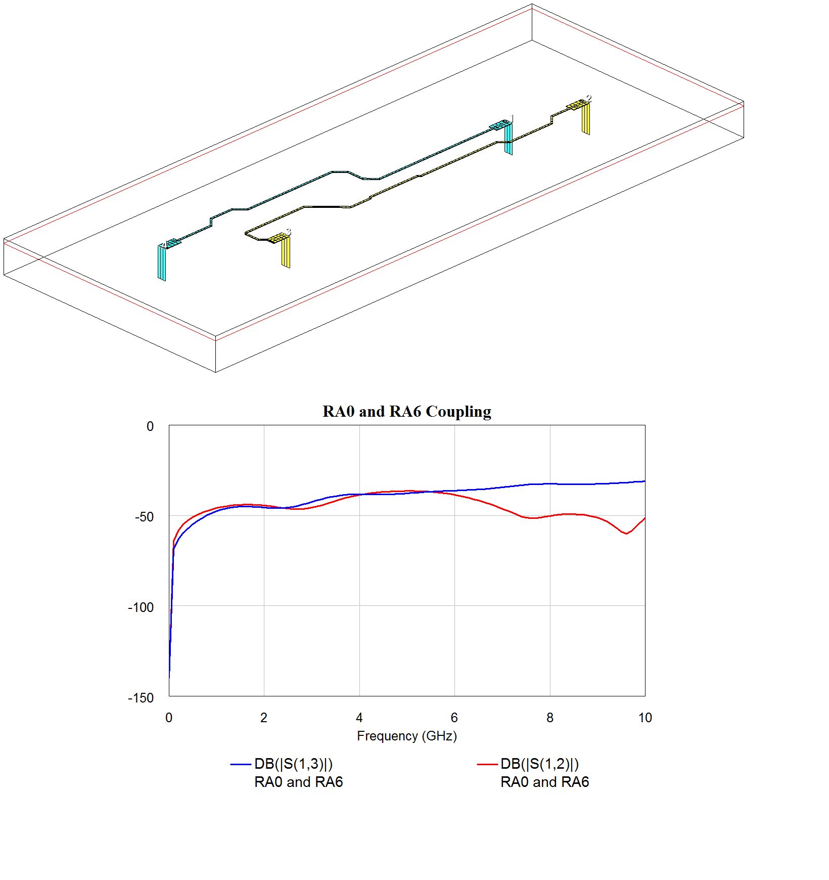
Importing PCB DataThe project will open and show the imported PA board layout, an EM structure created from the imported layout, and simulation results. Unfortunately this public domain demo board is not an RF or microwave design. We're working on finding a more realistic example, but, in the meantime, this board is sufficient for showing the PCB import flow. The optional steps below provide more detail on PCB import and setting up the EM structure from the imported data by walk through re-creating the data in this project. Alternatively, you may want to just look around the project as it stands and not worry about the detailed steps. |
 |
|
|
|
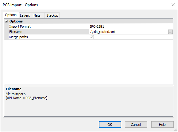
PCB Import WizardCloses all the open windows so that there is no clutter during the import process.
|
 |
|
|
|
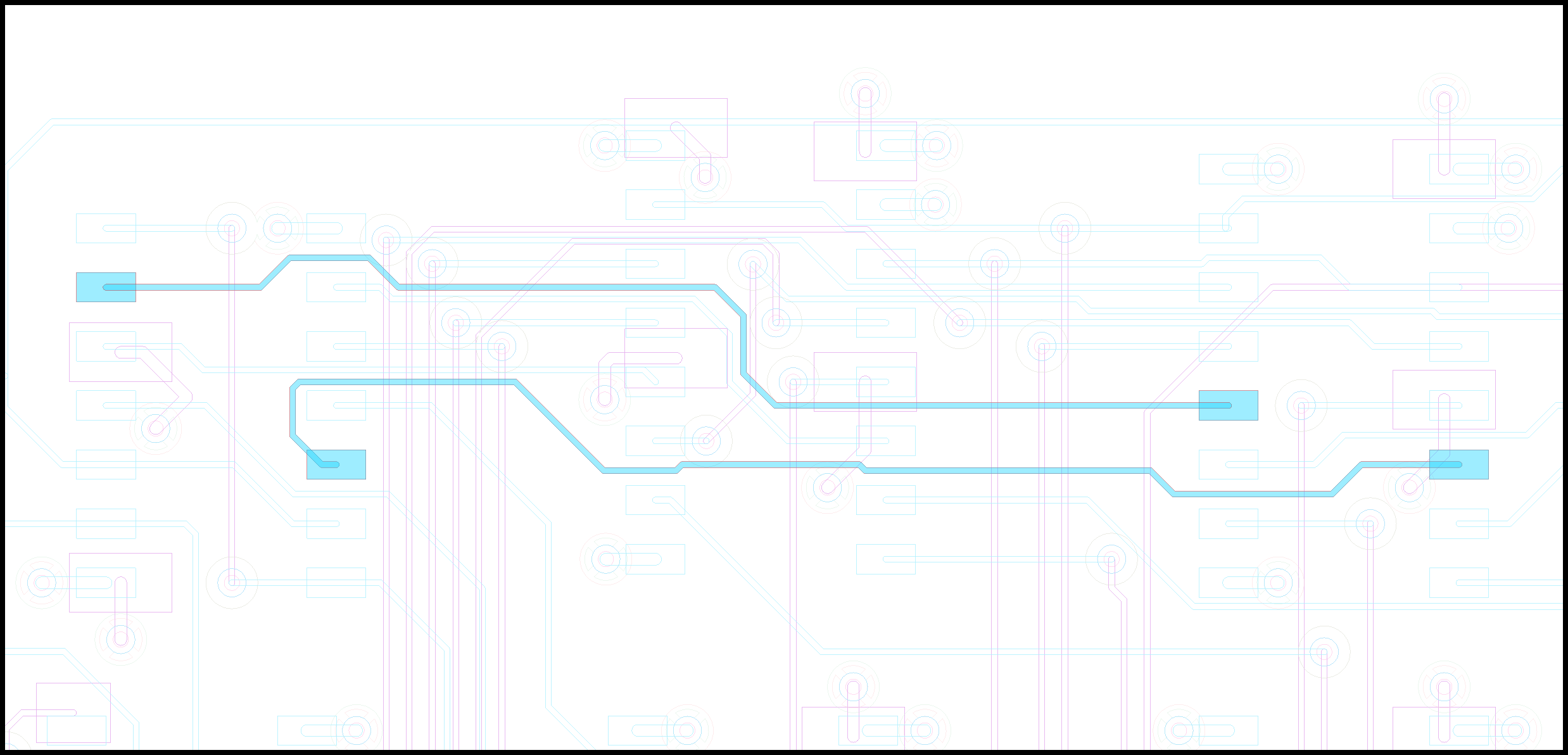
Selecting Nets and Configuring EM Clip RegionEntire nets can be selected by clicking on a shape in the layout, right clicking, and choosing Select By Name or with Edit > Select By Name. This example uses the latter approach.
EM Clip Regions (i.e. cutting out area around the nets) are auto-defined as a bounding boxes, convex hull, or concave hull with an expansion distance by choosing Draw > Create EM Clip Region or by drawing any shape and converting it to an EM Clip Region. This example doesn't use clip regions because the design is clearly digital with almost perfect ground planes so it seemed that clip regions would only add unnecssary complexity to the EM Structure |
 |
|
|
|
Creating EM Document
|
 |