These pages use active content which needs to be enabled in the AWR Design Environment by choosing Help > Enable Guided Help. Additional information can be found in the troubleshooting link on the bottom of each page.
|
|
|

|
|
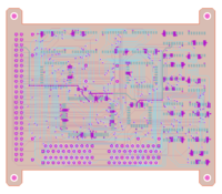
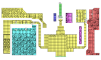
Quickly import PCB layout for EM analysis. |
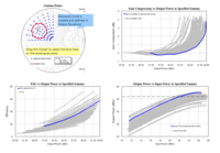
Increase device insight with source pull, harmonic load pull, and modulated signal analysis. |
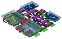
Easily create multi-technology designs, including Cadence Virutoso subcircuits. |
Design better filters by controlling stop-band nulls, pass-band edge asymmetry, and improved element order control. |
|
|
|
|
|
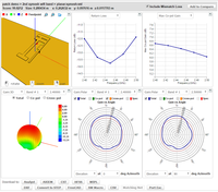
Synthesize antennas from easy-to-set-up specifications. |
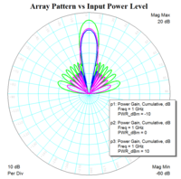
Efficiently simulate large phased arrays and design 5G MIMO systems. Discover the impact of phased arrays on system performance. |
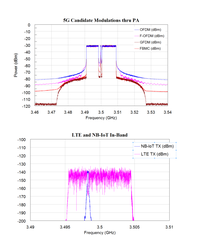
Jumpstart RF design using preconfigured 5G test benches and climb up the 5G learning curve quickly! |
Explore the design space with new optimization methods and synthesis wizards, perform carrier aggregation simulations, and share VSS data with your design team. |
|
|
|
|
|
See data more quickly with live simulation results and explore results intelligently with markers that lock to metrics. |
Eliminate manual re-entry by sending silicon design schematics back and forth to Cadence Virtuoso. |
Save schematic entry time with named nodes on S-parameter block and element parameter frames that no longer place in front of component pins. |
Reduce multiple test benches to one with the ability to make 2-port measurements like noise figure or max gain on N-port networks. |
|
|
|
|
|
Easily interact wtih multi-layer line types, save clicks with new editing commands, leverage the power of shape pre-processing and see more clearly with 2D translucency. |
Save tedious clicks with automatic port placement and simulate direclty in HFSS from Microwave Office. |
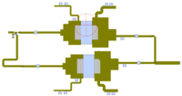
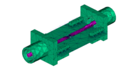
Efficiently manage complex 3D EM structures. |
|
Faster Answers |
Better Answers |
Minor Improvements |
New Stuff |